Blog
2023-01-08
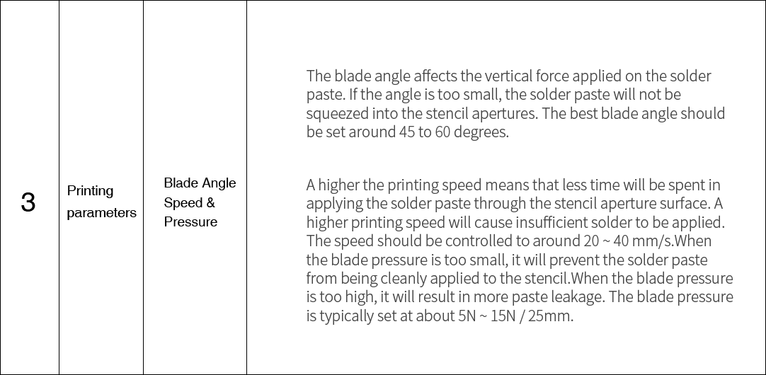
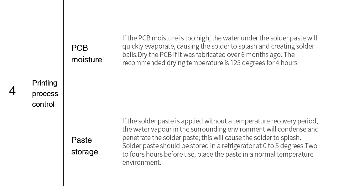
In SMT PCB production, solder paste printing is a critical step. Since the solder paste is used to directly form the soldering joint, the quality of solder paste printing affects the performance and reliability of the surface mount assembly. Quality solder paste printing guarantees a quality solder joint and final product. Statistics demonstrate that 60% to 90% of soldering defects are related to solder paste printing defects. So it is very important to understand what causes defects in solder paste printing.The following table lists an analysis of solder paste printing defects.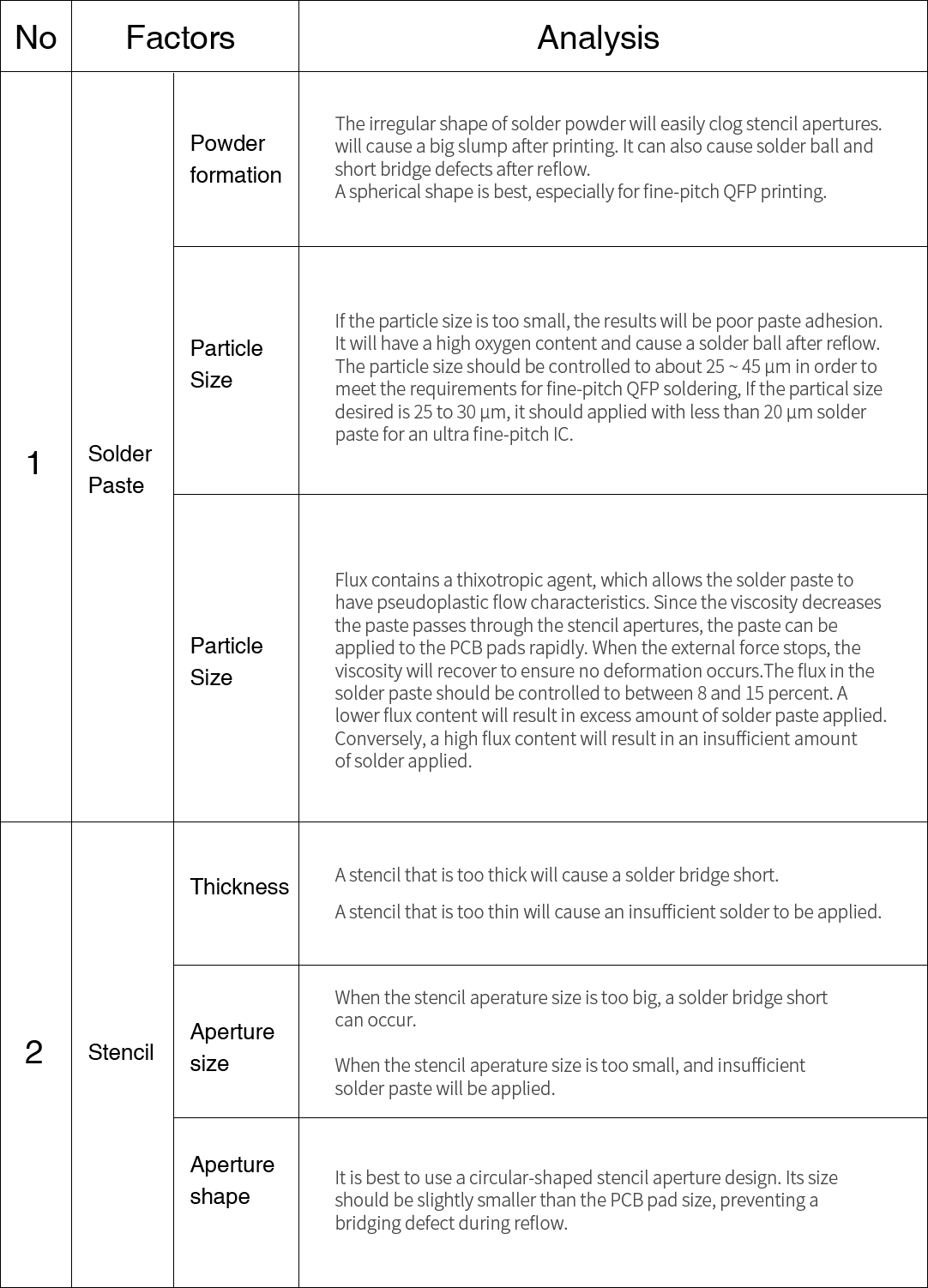
 图片宽度:700px, 图片高度:386px图片宽度:700px, 图片高度:343px
2023-01-08
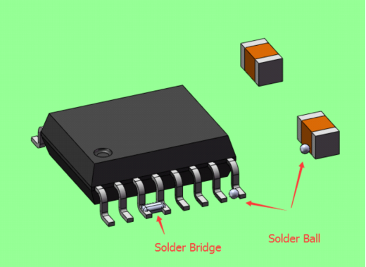 图片宽度:520px, 图片高度:379px
A solder ball is the most common type of defect that occurs in the SMT assembly process. Solder balls located within 0.13mm of traces violate the minimum electrical clearance principle. They can adversely affect the electrical reliability of the assembled PCB.
The following table lists an analysis of solder paste printing defects
According to the IPC A 610 standard, a PCB is also considered defective when there are 5 solder balls (<=0.13mm) within 600mm^2.
Analysis of Root Causes The solder ball is very closely related to air or water (trapped in solder paste) vapour escaping from the paste and turning into liquid. If the vapor in solder paste escapes too fast, a small amount of liquid solder will be taken from from soldering joint, and a solder ball will be formed when it cools down.
* PCB contains water.* Stored in an unexpectedly humid environment and isn’t dried before assembly.* PCB is too new and was not dried enough.* Too much flux is applied in the solder paste.* The preheat temperature is not high enough, so the flux has failed to effectively vapour out;* A solder paste printing issue due to the stencil not being clean, which causes the solder paste to stick to unexpected areas.Corrective Actions* Design the correct pad sizes and spaces according to the recommendation specified in the data sheet.* Reflow profile – when appropriate increase the preheating temperature.* Bake the PCB before printing.* PCB quality — The thickness of PCB hole’s plating copper is greater than 25μm in order to avoid trapping water in the PCB.Solder Bridging is another common defect, which occurs when the solder has formed an abnormal connection between two or more adjacent traces, pads or pins, and forms a conductive path.Analysis of Root Causes* There is no solder mask between adjacent pads.* The pads are spaced too close to one another.* There are residues stuck on the PCB surface or pads.* A dirty stencil with paste sticking on its underside.* A misalignment during solder paste printing* A misalignment when components are placed on the board.* Too high placement pressure will squeeze the paste out of the pads.* Paste slump has occurred or too much paste is applied to the pads.* The preheat temperature is not high enough, so the flux has not activated.Corrective Action* Add solder mask between the pads* Design the pads and stencil aperture to the right size.* Do not mix old and new flux together.* Adjust the solder paste printing pressure.* Adjust the pressure for pick and place nozzles.* Ensure there is a zero print gap between the PCB and the stencil.* Clean the stencil as quickly as possible.Corrective Action* Add solder mask between the pads* Design the pads and stencil aperture to the right size.* Do not mix old and new flux together.* Adjust the solder paste printing pressure.* Adjust the pressure for pick and place nozzles.* Ensure there is a zero print gap between the PCB and the stencil.* Clean the stencil as quickly as possible.Solder Bridging is another common defect, which occurs when the solder has formed an abnormal connection between two or more adjacent traces, pads or pins, and forms a conductive path.2023-01-28
The importance of testing in PCB manufacturing cannot be overstated. With PCBs being used for mission critical operations, the integrity & smooth functioning of the PCB is central to the efficacy of the device.One of the important tests to check whether the PCB has any manufacturing faults is Automated Optical Inspection or what is popularly known as AOI.What is Automated Optical Inspection(AOI)?Essentially as its name suggests, it is a machine-based technique that checks the PCB for any potential defects such as: – Surface Defects– Dimensional Defects– Component Placement DefectsWith complex circuit boards and boards being manufactured in large quantities, manual checking becomes more & more difficult. AOI therefore has emerged as an important tool to check efficacy of the board at cost effective price points. Let us look at how it really works.How exactly does AOI work? Essentially the process works as follows. A first article PCB is manually inspected. Found good, it is established as a “golden” unit. The AOI then learns from this unit what the gold standard is, in terms of various aspects such as component placement, solder joints and more. This information is then stored in its database. The AOI system then compares each new board with this unit & alerts the operators in case of any inconsistency. The AOI system is equipped with high-resolution cameras, which capture a wide array of images, which come in handy for the comparisons. Different equipment works well for different kinds of inspection. So, while solder paste inspection is done by way of laser scanning, an assembly verification system relies on imaging.Some of the methods that AOI makes use of, include: Template matching – Simply put, this is a pixel-by-pixel method, where a small template is applied to a large inspection image. Normalized Cross Correlation is then calculated between the template & inspection image.Object recognition – This method simply relies on a comparison between the ideal image & the captured imageBlob analysis – This involves separating the object from the background & then generating a blob by grouping object pixels.How exactly does AOI work? Miniaturization With the increasing trend of miniaturization, the size of PCB components is constantly on the decline and component density is high. In such a scenario, AOI comes in extremely handy in checking for the positional accuracy of components. The advantage with AOI is that it can detect even small deviations in position eliminating chances of a defect.Versatility The big advantage with AOI is that it is useful not only in case of PCB fabrication but also in PCB assembly where it helps in checking for aspects such as soldering and polarity. The fact that AOI can be used at any stage makes it an ever so important tool when it comes to inspection efficacy.Data collection & Retrieval AOI also helps in collection & retrieval of data which can take different formats such as image, data, text & more.Cost Advantage That AOI can help detect any manufacturing defects & save you from costly errors at a later date, makes it an extremely cost-effective process.Let us also look at some of the defects that AOI can help check. These are on the spectrum of both Fabrication & Assembly.Assembly:Inspection of solder paste.Finished solder joints.Checking the alignment of componentsPolarity indicators for component orientation.Marking of componentsLocation of fiducials.Labels as well as other markings.Fabrication:-Shorts-Any violations in trace width-Spacing violations-Excess copper-Missing component footprint pads.Drilled hole breakouts in PCB padsWith the ability to capture a wide range of defects, little surprise then that AOI finds wide application. What it offers is both quick & accurate inspection of errors and thereby it ensures high quality PCBs. Right from bare circuit boards to the SMT Assembly line, its importance is therefore ubiquitous.JINGHUA is one of the leading PCB manufacturers in CHINA, providing custom, lead-free and RoHS compliant PCB manufacturing solutions. Whether your requirement is for prototypes or large production runs, we have you covered.An overview of PCB testing and inspection methodsPCB is the basic component of any electronic circuit, simple or complex it may be. The wide use of surface mount components (SMD), combined with the need for multiple layers, has inevitably increased the complexity of today’s PCBs. Regardless of the application, the common requirement that all PCBs must meet is to function correctly according to the project specifications and to be free from defects. The latest generation electronic circuits include hundreds of components with thousands of welds and interconnections: it is, therefore, essential to define rigorous inspection and test procedures, capable of ensuring the quality of the final product. As a result of the reduced time-to-market and high competition in many electronics fields, some electronic circuits might exit the prototyping stage with bugs or defects that shall be identified and resolved before the product reaches the final stage.Overview of PCB testingWhen electronic circuits were relatively simple, manual visual inspection (MVI) was sufficient to detect potential issues such as short circuits, imperfect solder joints, interrupted traces, reverted polarity of some components, or even missing components. However, the MVI technique was not without problems related to the mistakes made by humans in performing boring and repetitive operations. This has created situations in which defects were not detected or were at a very advanced stage of the design, in which modifications to the circuit had become too expensive. The next step was to automate the visual inspection process using the AOI (Automated Optical Inspection) technique. AOI is now a proven inspection method, widely used both during welding preflow and welding postflow, and available on several pick-and-place machines. The increasingly massive use of SMD components and BGA (Ball Grid Array) packages have highlighted the limitations of AOI, no longer able to detect the connections and welds hidden underneath the package. The AXI (Automated X-ray Inspection) technique was thus developed, based on the use of X-rays capable of not only seeing through the package but also of inspecting multi-layer PCBs with a high density of components. Once the inspection phase has passed, the PCB shall undergo an accurate test, performed on the completely assembled circuit.Objective of PCB testingA PCB is made up of different elements, each of which affects the overall performance of the electronic circuit. The minimum set of tests to be performed should include the following checks:Electrical conductivity, including measurement of leakage currents;Mechanical resistance;Welds quality;Cleanliness (weather resistance, including humidity and corrosion);Quality of hole wall;Lamination, which tests the laminate’s resistance to peeling by force or application of heat; Copper plating, tested with tensile strength and analyzing the resulting elongation; Environmental test, especially for PCBs which operate in humid environments; Component polarity, orientation, alignment, and placement.AOIBeing an inspection method, AOI can detect PCB faults or defects at early development stage. AOI is a visual inspection method which uses cameras to acquire images of the board from different angles and with different lighting conditions. This technique also integrates OCR functionality capable of interpreting the serigraphs on the PCB. Acquired images are then compared with what one would like to achieve (the so-called “golden board”). This method has the advantage of detecting different types of defects and can be used in several development stages. The main disadvantage is that of being limited to a line of sight control, not able to check connections hidden by BGA or other types of packages.AXIThe high density introduced by SMT technology and the inability to identify connections in BGA and CSP (Chip Scale Package) packages, required more accurate inspection methods, such as those based on X-ray (AXI). Since welds are made with material whose atomic weight is higher than that of the other components on the board, they are clearly visible in the radiographic images. The main advantage of the AXI technique is that it detects all the connections and welds, even those hidden by the package; in addition, solder joints can also be inspected, highlighting the possible presence of bubbles. The chance of detecting any counterfeits of proprietary electronic components is also significant. On the other hand, AXI is a relatively expensive technique, the investment of which can be justified only for high density PCBs and components with BGA or CSP package. Figure 1 shows a defect detected by X-ray inspection.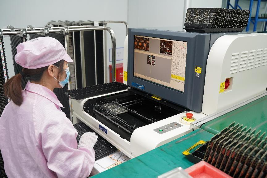 Figure 1: PCB defect detected by X-ray inspectionIn-circuit test (ICT)
This test, performed after the assembly stage, verifies the correct functioning and position of each electronic component on the PCB. The test includes verification of short circuits, open circuits, resistance, capacitance and other parameters. For this purpose, a flying probe is used, composed of an array of drivers and sensors that perform the measurements required by the test by moving freely on the board. The probe is controlled by appropriate software, which can be modified by adapting the same test system to boards with different layouts. Alternatively, a test fixture can be used, consisting of a bed of nails designed for the specific DUT (Device Under Test). Each “nail” behaves like a real sensor, able to electrically connect a specific point of the DUT to the test system. Bed-of-nails is an expensive and not very flexible technique (each board requires its own bed-of-nails); moreover, it shows some difficulties in testing boards with high component density, where spacing between pins is reduced. The ICT technique has the advantage of detecting several defects, relating to both the individual components and their connections, and can be performed without powering the board. Its disadvantage is related to the cost (complexity of both bed-of-nails and control software) and the inability to test the connectors, a significant limitation in analog and digital systems consisting of multiple cards. Figure 2 shows an ICT test machine with a flying probe.