JinHua Tech has developed a complete and advanced PCB testing procedure and quality control system to ensure our PCB production features good performance and stability. Different PCB boards have different PCB test requirements and PCB test methods. Customers provide test software, parameters and technical guidance, we will prepare different test fixtures and equipment according to customers’ test requirements. Our QA will complete the final PCB functional test to meet the designer’s requirements. The functional tests include: ICT test, FCT test, aging test, fatigue test, etc.
DFM Check
DFM test detects the unreasonable PCB design before mass production. It optimizes the processing of GERBER information, making customer’s PCB design into reality. It can also find the problem in advance to promote the PCB production, reduce the risk of scrap, and improve the one-time pass rate, especially for batch PCB orders.
ERP System
ERP system is a positive platform to control the whole production process. All the entire PCB production process data are be recorded in the system, easy and transparent to follow up and trace the process. If one of the production links has problems, we can quickly find out and solve them.
Incoming Material Inspection (IQC)
Our IQC will strict test PCB boards, including inspections on components, PCBs and other materials:
Reflow oven temperature test/ No flying lines/Whether the holes are blocked or leaking ink/Whether the board surface is bent, etc.
Checking whether the model, brand and quantity match/Whether they are genuine (the components used by our company must be genuine, imitations and inferior products cannot pass the inspection)
Pin number and spacing check: plugs, IC, connectors, buttons, inductors, etc.
IQC will combine the PCB screen printing characters.
PAD bit to check the number of PIN pin, PIN pin spacing is matched to ensure that the incoming materials are correct.
Online SPI inspection of solder paste quality
To meet the requirements of high quality, PCB boards are randomly tested under the online SPI inspection. SPI checks solder paste volume, area, height, shape, offset, even tin, more tin, less tin, even tin, pull tip, collapse, and shapes. If the PCB boards can not pass SPI inspection, they will not flow to the next process to patch, and rework cleaning re-brush solder paste.
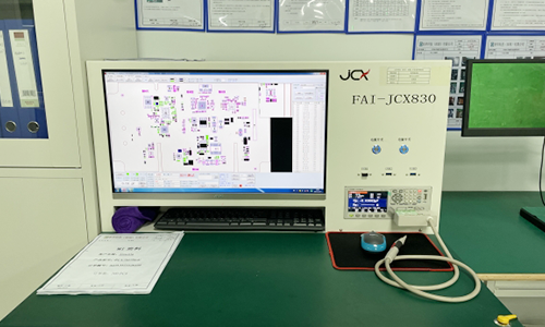
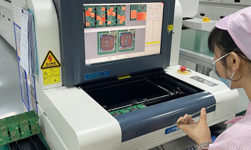
First PCB piece test before reflow soldering
First piece tester integrates CAD coordinates, BOM list and first piece PCB board scan map. This system automatically enters the measurement data, with LCR automatically reading the relevant data and judge the PCB test results. The first piece tester can generate test reports, helping eliminate mismeasurement and missed tests. If there is any problem, we will stop the line, material, debugging machine parameters, and then cycle the first production test process.
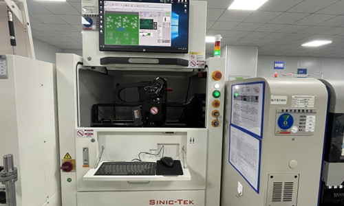
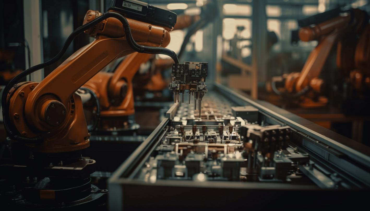
AOI Inspection
AOI automatically scans the PCB and collects images through the camera. By comparing the tested solder joints with the qualified parameters in the database, and image processing, the defects on the PCB can be effortlessly checked, which are displayed/marked out through the monitor or automatic signs, good for maintenance personnel to fix.
X-RAY inspection
X-ray inspection mainly tests internal defects in solder joints, and some precisive devices such as BGA, CSP and Chip. It has a strong penetrating properties, penetrating the surface of the object, the inside of the inspected solder joints. The X-ray inspection can detect and analyze the solder quality of various solder joints of electronic components, including open circuit, short circuit, holes, holes, internal bubbles and insufficient amount of tin, It can also detect solder joint defects such as bridging, open circuits, lost solder balls, displacement, insufficient brazing material, voids, solder balls and blurred solder joint edges internally under the BGA package device.
Wherever you are located in the world – please feel free to ask us anything from a technical question to a quote.

Jinhua, a top Chinese PCB manufacturer, produces cutting-edge electronics products, PCB prototype, PCB, PCB assembly, PCB fabrication service & more. Your trusted one-stop solution for PCB, making the effective and easy way.
Jinhua Technology (Shenzhen) Co., Ltd. All rights reserved.